- 您现在的位置:买卖IC网 > Sheet目录328 > IDT709149S10PFI (IDT, Integrated Device Technology Inc)IC SRAM 36KBIT 10NS 80TQFP
�� �
�
�IDT709149S�
�High-Speed� 36K� (4K� x� 9-bit)� Synchronous� Pipelined� Dual-Port� Static� RAM�
�Industrial� and� Commercial� Temperature� Ranges�
�DC� Electrical� Characteristics� Over� the� Operating�
�Temperature� and� Supply� Voltage� Range� (4)� (V� CC� =� 5V� ±� 10%)�
�709149S8�
�Com'l� Only�
�709149S10�
�Com'l�
�&� Ind�
�709149S12�
�Com'l� Only�
�Symbol�
�I� CC�
�I� SB1�
�Parameter�
�Dynamic� Operating�
�Current�
�(Both� Ports� Active)�
�Standby� Current�
�(Both� Ports� -� TTL�
�Level� Inputs)�
�Test� Condition�
�CE� L� and� CE� R� =� V� IL� ,�
�Outputs� Disabled�
�f� =� f� MAX� (1)�
�CE� L� and� CE� R� =� V� IH�
�f� =� f� MAX� (1)�
�Version�
�COM'L�
�IND�
�COM'L�
�IND�
�Typ.�
�200�
�____�
�100�
�____�
�Max.�
�320�
�____�
�150�
�____�
�Typ.�
�190�
�190�
�90�
�90�
�Max.�
�310�
�340�
�150�
�175�
�Typ.�
�180�
�____�
�85�
�____�
�Max.�
�300�
�____�
�140�
�____�
�Unit�
�mA�
�mA�
�I� SB2�
�Standby� Current�
�CE� "A"� =� V� IL� and� CE� "B"� =� V� IH�
�(3)�
�COM'L�
�180�
�230�
�170�
�220�
�160�
�210�
�mA�
�(One� Port� -� TTL�
�Level� Inputs)�
�Active� Port� Outputs� Disabled,�
�f=f� MAX� (1)�
�IND�
�____�
�____�
�170�
�250�
�____�
�____�
�I� SB3�
�I� SB4�
�Full� Standby� Current�
�(Both� Ports� -� All�
�CMOS� Level� Inputs)�
�Full� Standby� Current�
�(One� Port� -� All�
�CMOS� Level� Inputs)�
�CE� L� and�
�CE� R� >� V� CC� -� 0.2V,�
�V� IN� >� V� CC� -� 0.2V� or�
�V� IN� <� 0.2V,� f� =� 0� (2)�
�CE� "A"� <� 0.2V� and�
�CE� "B"� >� V� CC� -� 0.2V� (3)�
�V� IN� >� V� CC� -� 0.2V� or� V� IN� <� 0.2V�
�COM'L�
�IND�
�COM'L�
�IND�
�5�
�____�
�170�
�____�
�15�
�____�
�220�
�____�
�5�
�5�
�160�
�160�
�15�
�20�
�210�
�240�
�5�
�____�
�150�
�____�
�15�
�____�
�200�
�____�
�mA�
�mA�
�Active� Port� Outputs� Disabled,�
�f� =� f� MAX� (1)�
�NOTES:�
�3494� tbl� 06�
�1.� At� f� =� f� MAX� ,� address� and� control� lines� (except� Output� Enable)� are� cycling� at� the� maximum� frequency� clock� cycle� of� 1/t� CLK� ,� using� "AC� TEST� CONDITIONS"� at� input� levels� of�
�GND� to� 3V.�
�2.� f� =� 0� means� no� address,� clock,� or� control� lines� change.� Applies� only� to� input� at� CMOS� level� standby.�
�3.� Port� "A"� may� be� either� left� or� right� port.� Port� "B"� is� the� opposite� from� port� "A".�
�4.� Vcc� =� 5V,� T� A� =� 25°C� for� Typ,� and� are� not� production� tested.� I� CC� DC� =� 150mA� (Typ).�
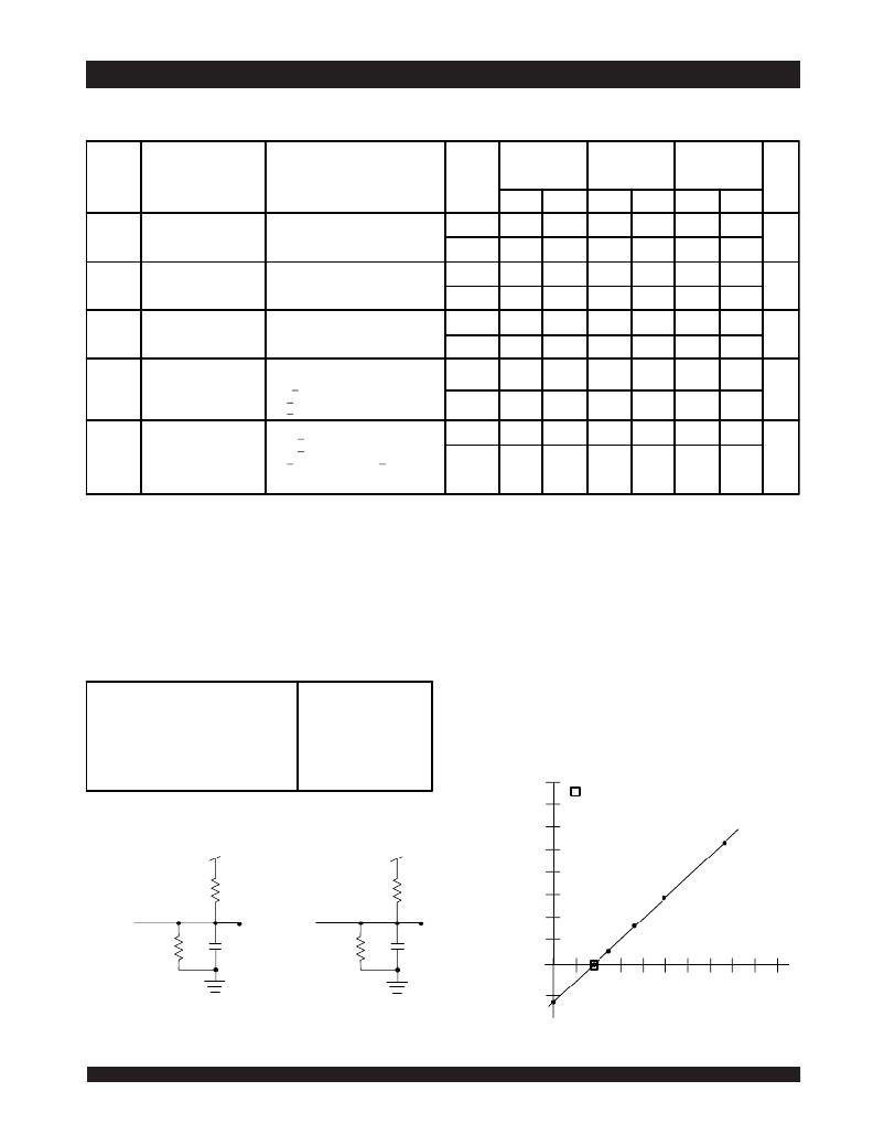
�AC� Test� Conditions�
�Input� Pulse� Levels�
�Input� Rise/Fall� Times�
�Input� Timing� Reference� Levels�
�Output� Reference� Levels�
�GND� to� 3.0V�
�3ns� Max.�
�1.5V�
�1.5V�
�Output� Load�
�Figures� 1,2� and� 3�
�3494� tbl� 07�
�8�
�7�
�9pF� is� the� I/O� capacitance�
�of� this� device,� and� 30pF� is� the�
�AC� Test� Load� Capacitance�
�6�
�DATA� OUT�
�5V�
�893� ?�
�DATA� OUT�
�5V�
�893� ?�
�?� tCD�
�(Typical,� ns)�
�5�
�4�
�3�
�2�
�347� ?�
�30pF�
�347� ?�
�5pF*�
�1�
�0�
�20� 40� 60� 80� 100� 120� 140� 160� 180� 200�
�,�
�3494� drw� 03�
�Figure� 1.� AC� Output� Test� load.�
�3494� drw� 04�
�Figure� 2.� Output� Test� Load�
�,�
�-1�
�Capacitance� (pF)�
�3494� drw� 05�
�(For� t� CKLZ� ,� t� CKHZ� ,� t� OLZ� ,� and� t� OHZ� ).�
�*Including� scope� and� jig.�
�6.42�
�Figure� 3.� Typical� Output� Derating� (Lumped� Capacitive� Load).�
�发布紧急采购,3分钟左右您将得到回复。
相关PDF资料
IDT70914S12PF
IC SRAM 36KBIT 12NS 80TQFP
IDT709169L7BFI
IC SRAM 144KBIT 7NS 100FBGA
IDT709279L9PFG
IC SRAM 512KBIT 9NS 100TQFP
IDT709289L9PFI
IC SRAM 1MBIT 9NS 100TQFP
IDT709359L7BFI
IC SRAM 144KBIT 7NS 100FBGA
IDT709379L7PFG
IC SRAM 576KBIT 7NS 100TQFP
IDT70P257L55BYGI
IC SRAM 128KBIT 55NS 100BGA
IDT70P258L55BYI
IC SRAM 128KBIT 55NS 100BGA
相关代理商/技术参数
IDT709149S10PFI8
功能描述:IC SRAM 36KBIT 10NS 80TQFP RoHS:否 类别:集成电路 (IC) >> 存储器 系列:- 标准包装:1,000 系列:- 格式 - 存储器:RAM 存储器类型:SRAM - 双端口,同步 存储容量:1.125M(32K x 36) 速度:5ns 接口:并联 电源电压:3.15 V ~ 3.45 V 工作温度:-40°C ~ 85°C 封装/外壳:256-LBGA 供应商设备封装:256-CABGA(17x17) 包装:带卷 (TR) 其它名称:70V3579S5BCI8
IDT709149S12PF
功能描述:IC SRAM 36KBIT 12NS 80TQFP RoHS:否 类别:集成电路 (IC) >> 存储器 系列:- 标准包装:1,000 系列:- 格式 - 存储器:RAM 存储器类型:SRAM - 双端口,同步 存储容量:1.125M(32K x 36) 速度:5ns 接口:并联 电源电压:3.15 V ~ 3.45 V 工作温度:-40°C ~ 85°C 封装/外壳:256-LBGA 供应商设备封装:256-CABGA(17x17) 包装:带卷 (TR) 其它名称:70V3579S5BCI8
IDT709149S12PF8
功能描述:IC SRAM 36KBIT 12NS 80TQFP RoHS:否 类别:集成电路 (IC) >> 存储器 系列:- 标准包装:45 系列:- 格式 - 存储器:RAM 存储器类型:SRAM - 双端口,异步 存储容量:128K(8K x 16) 速度:15ns 接口:并联 电源电压:3 V ~ 3.6 V 工作温度:0°C ~ 70°C 封装/外壳:100-LQFP 供应商设备封装:100-TQFP(14x14) 包装:托盘 其它名称:70V25S15PF
IDT709149S8PF
功能描述:IC SRAM 36KBIT 8NS 80TQFP RoHS:否 类别:集成电路 (IC) >> 存储器 系列:- 标准包装:1,000 系列:- 格式 - 存储器:RAM 存储器类型:SRAM - 双端口,同步 存储容量:1.125M(32K x 36) 速度:5ns 接口:并联 电源电压:3.15 V ~ 3.45 V 工作温度:-40°C ~ 85°C 封装/外壳:256-LBGA 供应商设备封装:256-CABGA(17x17) 包装:带卷 (TR) 其它名称:70V3579S5BCI8
IDT709149S8PF8
功能描述:IC SRAM 36KBIT 8NS 80TQFP RoHS:否 类别:集成电路 (IC) >> 存储器 系列:- 标准包装:1,000 系列:- 格式 - 存储器:RAM 存储器类型:SRAM - 双端口,同步 存储容量:1.125M(32K x 36) 速度:5ns 接口:并联 电源电压:3.15 V ~ 3.45 V 工作温度:-40°C ~ 85°C 封装/外壳:256-LBGA 供应商设备封装:256-CABGA(17x17) 包装:带卷 (TR) 其它名称:70V3579S5BCI8
IDT70914S12J
功能描述:IC SRAM 36KBIT 12NS 68PLCC RoHS:否 类别:集成电路 (IC) >> 存储器 系列:- 标准包装:1,000 系列:- 格式 - 存储器:RAM 存储器类型:SRAM - 双端口,同步 存储容量:1.125M(32K x 36) 速度:5ns 接口:并联 电源电压:3.15 V ~ 3.45 V 工作温度:-40°C ~ 85°C 封装/外壳:256-LBGA 供应商设备封装:256-CABGA(17x17) 包装:带卷 (TR) 其它名称:70V3579S5BCI8
IDT70914S12J8
功能描述:IC SRAM 36KBIT 12NS 68PLCC RoHS:否 类别:集成电路 (IC) >> 存储器 系列:- 标准包装:45 系列:- 格式 - 存储器:RAM 存储器类型:SRAM - 双端口,异步 存储容量:128K(8K x 16) 速度:15ns 接口:并联 电源电压:3 V ~ 3.6 V 工作温度:0°C ~ 70°C 封装/外壳:100-LQFP 供应商设备封装:100-TQFP(14x14) 包装:托盘 其它名称:70V25S15PF
IDT70914S12PF
功能描述:IC SRAM 36KBIT 12NS 80TQFP RoHS:否 类别:集成电路 (IC) >> 存储器 系列:- 标准包装:1,000 系列:- 格式 - 存储器:RAM 存储器类型:SRAM - 双端口,同步 存储容量:1.125M(32K x 36) 速度:5ns 接口:并联 电源电压:3.15 V ~ 3.45 V 工作温度:-40°C ~ 85°C 封装/外壳:256-LBGA 供应商设备封装:256-CABGA(17x17) 包装:带卷 (TR) 其它名称:70V3579S5BCI8